ProductsProducts
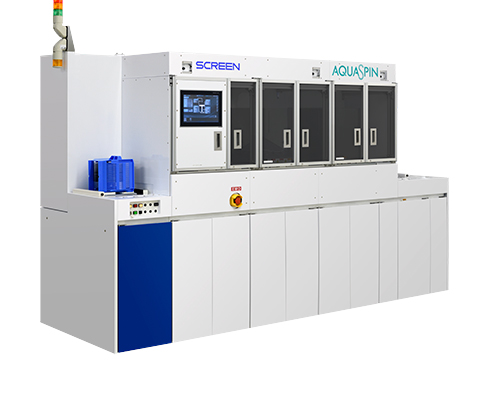
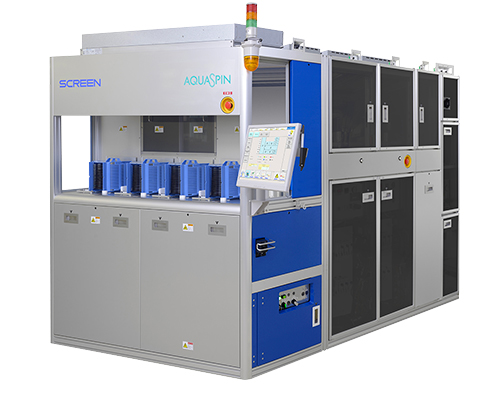
Spin Processor
SP-2100
Wafer size 76mm ~ 200mm
Outstanding functionality and scalability easily handle emerging needs
-
1. Reliable wafer transfer using a mechanical method
The SP-2100 employs an I-LINE single path transfer system. Stable wafer transfer is achieved by a pick-and-place method of mechanical transfer with a well-established track record.
-
2. Suitable for a wide range of compound wafers
The SP-2100 is suitable for SiC, GaN, LiTaO3, and many other types of compound wafers, as well as silicon wafers. It can process a wide range of wafer sizes from 76 to 200 mm.
-
3. Processing chamber (MTC/DTC)
Multitask chamber
The SP-2100 can also perform cleaning and etching using high-temperature strong acids.Dry-task chamber
Wafers are rinsed using DIW, followed by high-speed spin drying. -
4. Suitable for metal etching processes
The SP-2100 can perform etching with high reproducibility when equipped with the optional SCREEN proprietary endpoint sensor.
-
5. A new GUI enhances usability
The SP-2100 features a new GUI and an updated control system for simple, intuitive operation.
-
6. Optional cleaning tools further expand device compatibility
Either Nanospray or Softspray is available as an optional cleaning tool, and a surface brush can also be installed for post-CMP cleaning and other processes. The SP-2100 can thus perform a wide range of cleaning processes to suit the purpose and application.
Other
-
Spin Scrubber
SS-80EX
Wafer size 100mm ~ 200mm
Advanced Scrubber Featuring the Same Stability and Reliability as the Highly Regarded SS Series.
-
Spin Processor
SU-2000
Wafer size 150mm ~ 200mm
Inherits High-end Single Wafer Cleaning Technology to Deliver Outstanding Cost Performance
-
Coat/Develop Track
SK-60EX/
SK-80EXWafer size 150mm ~ 200mm
Flexibility to Process a Variety of Substrates